> For the complete documentation index, see [llms.txt](https://170th-street.gitbook.io/hx/llms.txt). Markdown versions of documentation pages are available by appending `.md` to page URLs; this page is available as [Markdown](https://170th-street.gitbook.io/hx/hardware/full-specifications.md).

# Full Specifications

This page documents every known specification of the NVIDIA CMP 170HX in one place. Where figures differ between sources, the most accurate measured values are used.

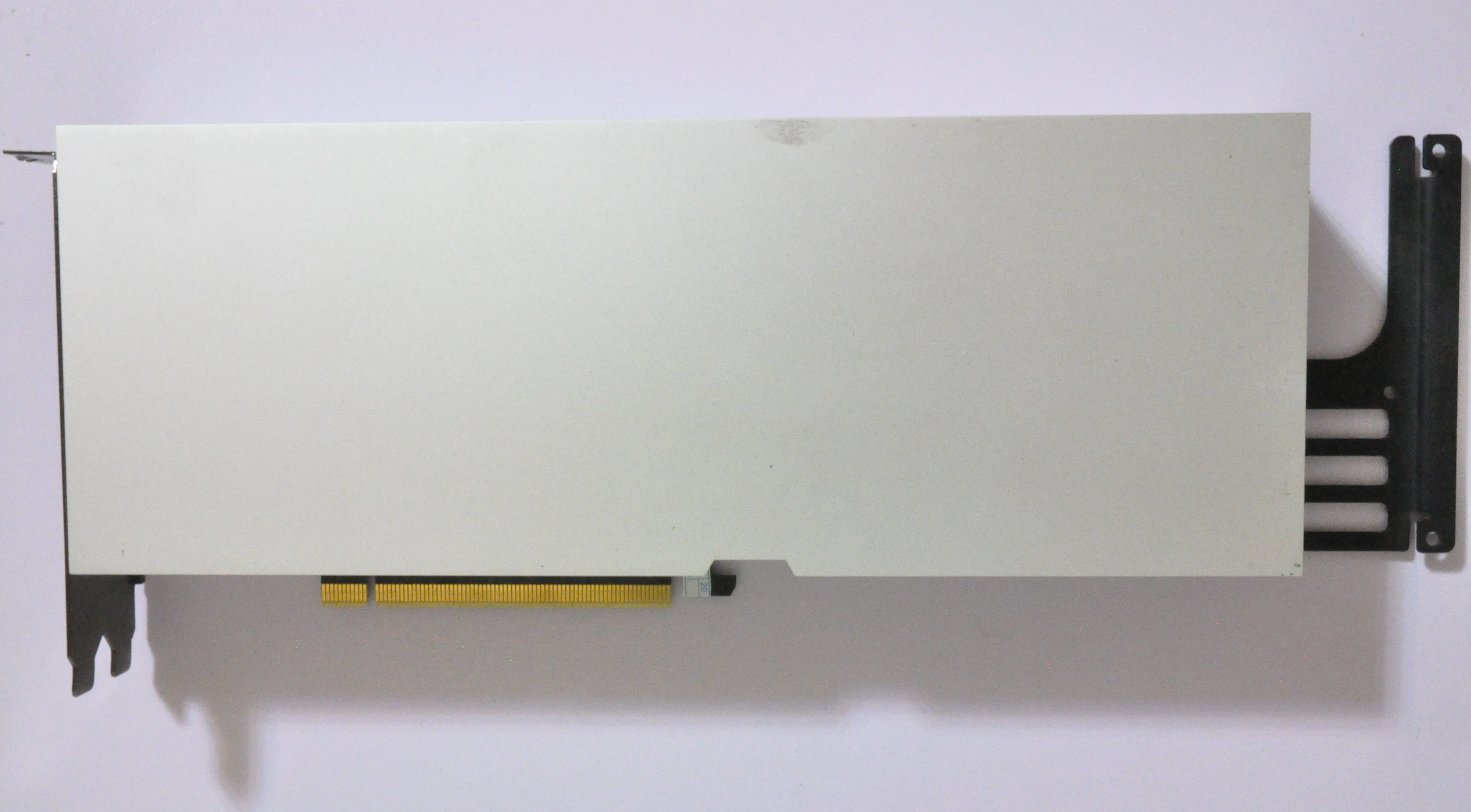
<figure><img src="https://niconiconi.neocities.org/img/nvidia-cmp-170hx-review/cmp-170hx-teardown-0.jpg" alt=""><figcaption></figcaption></figure>

**General**

| Property              | Value                                      |
| --------------------- | ------------------------------------------ |
| Model                 | NVIDIA CMP 170HX                           |
| GPU Die               | GA100-105F-A1 (8GB) / GA100-105A-A1 (10GB) |
| Architecture          | Ampere                                     |
| Manufacturing Process | TSMC 7nm N7 FinFET                         |
| Transistors           | 54.2 billion                               |
| Die Size              | 826 mm²                                    |
| **PCI Device ID**     | **0x20C2 (8GB) / 0x2082 (10GB)**           |
| **PCI Subsystem ID**  | **0x1585 (8GB) / 0x1557 (10GB)**           |
| Release Date          | September 1, 2021                          |
| Original MSRP         | $4,299 USD                                 |
| Form Factor           | Dual-slot PCIe add-in card                 |
| Cooling               | Passive                                    |
| Display Outputs       | None                                       |

**Compute**

| Property                       | Value             |
| ------------------------------ | ----------------- |
| Streaming Multiprocessors (SM) | 70                |
| CUDA Cores                     | 4,480 (64 per SM) |
| Tensor Cores (3rd Generation)  | 280 (4 per SM)    |
| Texture Units (TMUs)           | 280               |
| Render Output Units (ROPs)     | 128               |
| Base Clock                     | 1140 MHz          |
| Boost Clock                    | 1410 MHz          |
| L1 Cache                       | 192 KB per SM     |
| L2 Cache                       | 32,768 KB (32 MB) |

**Memory**

<table><thead><tr><th>Property</th><th width="367">Value</th></tr></thead><tbody><tr><td>Memory Type</td><td>HBM2e</td></tr><tr><td>Memory Capacity</td><td>8 GB / 10 GB</td></tr><tr><td>Unlocked Memory Capacity</td><td>64GB (8GB) / 40GB (10GB)</td></tr><tr><td>Memory Bus Width</td><td>4,096-bit (8GB) / 5,120-bit (10GB)</td></tr><tr><td>Memory Clock</td><td>1,458 MHz (8GB) / 1215 MHz (10GB)</td></tr><tr><td>Memory Bandwidth (theoretical)</td><td>1.49TB/s (8GB) / 1.56TB/s (10GB)</td></tr><tr><td>ECC</td><td>Disabled</td></tr><tr><td>Resizable BAR</td><td>Present but limited to 64 MiB</td></tr></tbody></table>

**Performance (Theoretical vs Actual)**

<table><thead><tr><th width="222">Metric</th><th width="256">Original</th><th width="255">Unlocked</th></tr></thead><tbody><tr><td>FP64</td><td>0.19 TLFOPS/s</td><td>6.44 TFLOPS/s</td></tr><tr><td>FP32</td><td>0.41 TLFOPS/s</td><td>12.99 TFLOPS/s</td></tr><tr><td>FP16</td><td>49.05 TFLOPS/s</td><td>49.05 TFLOPS/s</td></tr><tr><td>INT64</td><td>2.52 TFLOPS/s</td><td>2.52 TFLOPS/s</td></tr><tr><td>INT32</td><td>12.99 TFLOPS/s</td><td>12.99 TFLOPS/s</td></tr><tr><td>INT16</td><td>11.94 TFLOPS/s</td><td>11.94 TFLOPS/s</td></tr><tr><td>INT8</td><td>1.64 TFLOPS/s</td><td>48.03 TFLOPS/s</td></tr></tbody></table>

**Connectivity**

| Property                    | Value                                          |
| --------------------------- | ---------------------------------------------- |
| PCIe Interface (physical)   | x16 slot                                       |
| PCIe Interface (electrical) | Gen 1 x4 (firmware locked)                     |
| PCIe Bandwidth              | \~1 GB/s                                       |
| NVLink                      | Physical connectors present, disabled via fuse |
| Power Connector             | 1× 8-pin CPU power connector (via adapter)     |

**Power**

| Property                   | Value    |
| -------------------------- | -------- |
| TDP (default)              | 250W     |
| Max Power Limit (software) | 300W     |
| Idle Power (typical)       | \~30–40W |

**API Support**

| API           | Supported                      |
| ------------- | ------------------------------ |
| CUDA          | ✅ Yes (Compute Capability 8.0) |
| OpenCL        | ✅ Yes (3.0)                    |
| DirectX       | ❌ No                           |
| Vulkan        | ❌ No                           |
| OpenGL        | ❌ No                           |
| NVENC / NVDEC | ❌ No                           |

<figure><img src="https://3020394378-files.gitbook.io/~/files/v0/b/gitbook-x-prod.appspot.com/o/spaces%2FSuB7E7HJrJNSOEniEoFs%2Fuploads%2FvJN1F0CyNhqZ6CPS5vFm%2F170HX%20Board.png?alt=media&amp;token=a148ef46-c83c-40c0-b72a-ee6dc7ae3f26" alt=""><figcaption></figcaption></figure>

**Notes on Specification Discrepancies**

The CMP 170HX exists in multiple hardware configurations: **8GB, and 10GB variants are confirmed real production cards**, not database errors. These are not merely software differences controlled by firmware; they represent genuine hardware binning variants with different memory configurations:

* **8GB variant:** 4,096-bit memory bus
* **10GB variant:** 5,120-bit memory bus
